Published · CERAMIC CNC Engineering · Engineering Guide · 8 min read
AI Semiconductor Equipment Ceramic Parts: Wafer Handling, Chucks, Micro-Holes
How AI-driven semiconductor equipment demand changes RFQ review for precision ceramic wafer handling parts, vacuum chucks, gas plates, SiC rings, and micro-hole components.
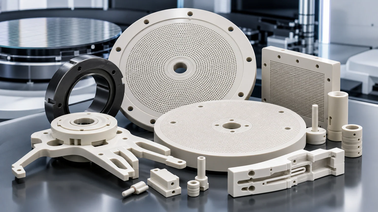
AI chip demand does not only increase demand for silicon. It also raises the precision burden on the ceramic parts inside wafer handling, vacuum, etch, deposition, inspection, and advanced packaging equipment.
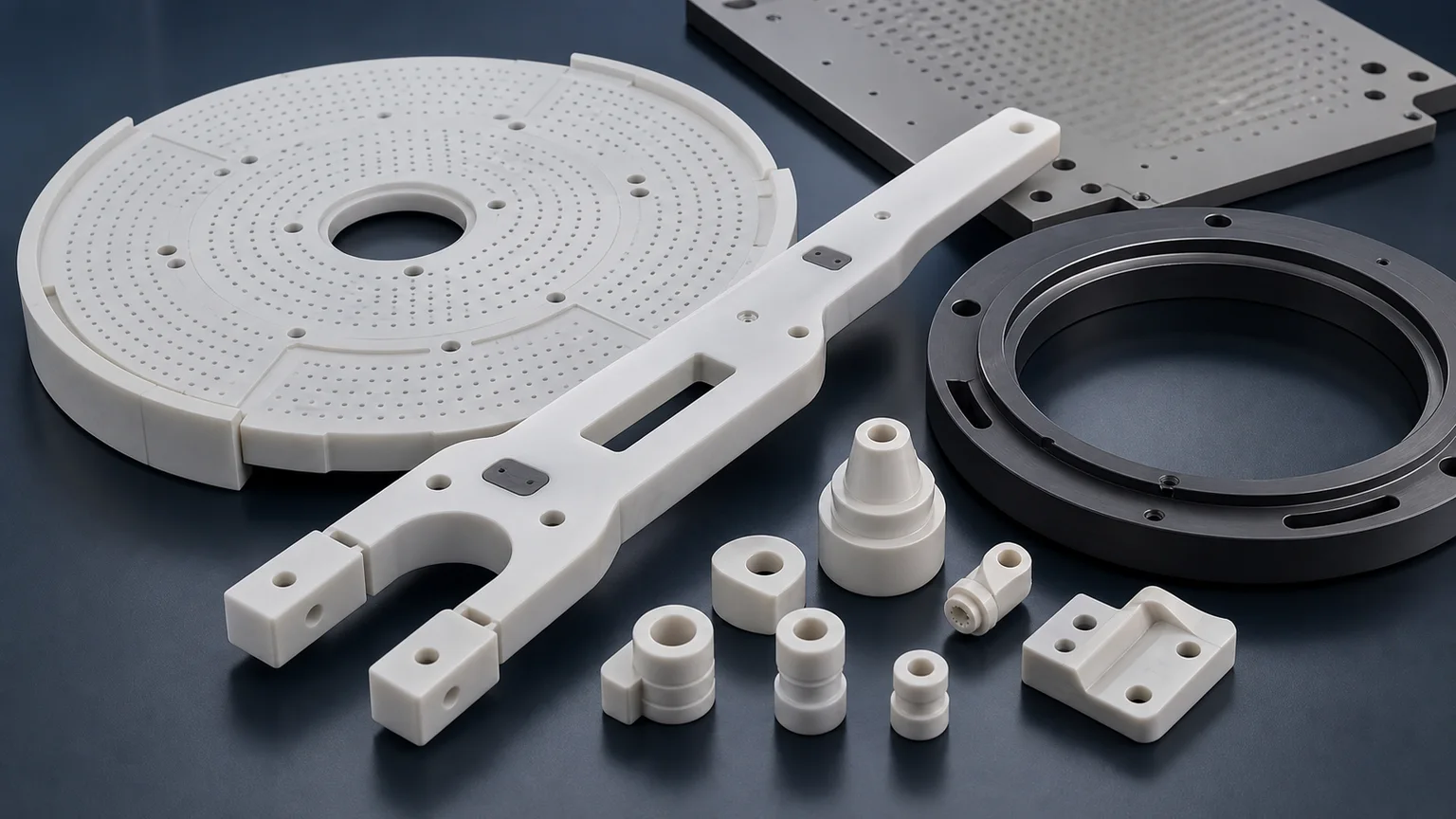
Semiconductor ceramic components are not purchased like ordinary ceramic plates. A wafer chuck, gas baffle, end effector, insulating spacer, nozzle, or SiC process-side ring may be judged by flatness, edge particle risk, hole uniformity, thermal stability, plasma exposure, and whether the inspection method can prove the feature that matters.
This article is written for engineering and sourcing teams preparing RFQs for ceramic CNC machining, diamond grinding, micro-drilling, and lapping work around semiconductor equipment components. It is not a promise that every semiconductor ceramic drawing can be quoted directly. It is a way to make the review package useful before price and schedule are confirmed.
For a component-by-component sourcing view, use the newer precision ceramic components for semiconductor equipment guide.
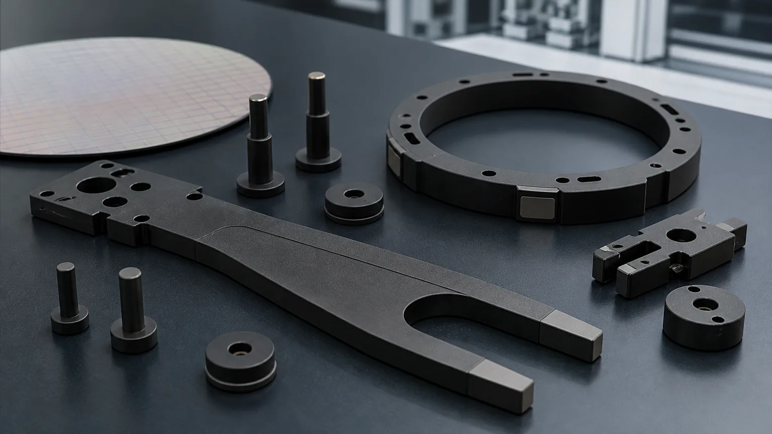
For SiC wafer handling blades, lift pins, support pads, and edge-contact parts, use the focused silicon carbide wafer handling components guide.
For ceramic fork blades, grippers, vacuum picks, support fingers, and robot mounting datums across multiple ceramic materials, use the ceramic end effectors for wafer handling guide.
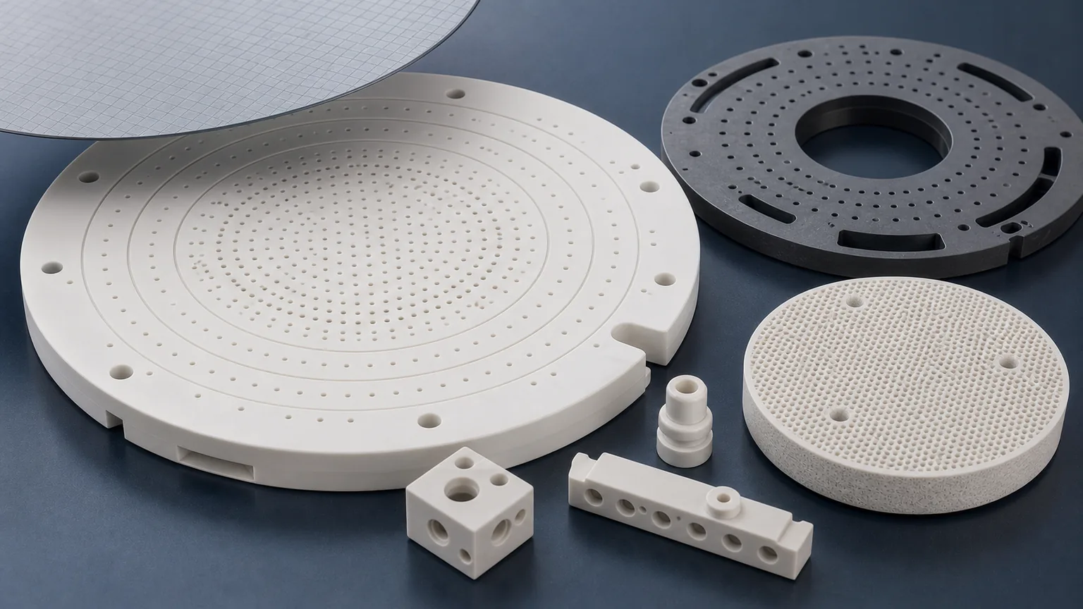
For dense and porous ceramic vacuum chuck plates, SiC chuck rings, hole fields, grooves, flatness maps, and vacuum evidence, use the machined ceramic vacuum chuck components guide.
For process chamber ceramic rings, SiC and alumina ring components, lapped annular bands, ID/OD control, groove edges, cleaning, and inspection evidence, use the precision ceramic rings for semiconductor process chambers guide.
For alumina insulating rings, AlN thermal insulators, feedthrough-adjacent sleeves, electrode spacers, creepage paths, plasma-adjacent edge quality, and deposition-tool cleaning requirements, use the ceramic insulators for plasma etching and deposition equipment guide.
For AlN heat spreaders, heater-adjacent plates, insulating thermal spacers, ceramic carriers, clean packaging, and thermal-interface inspection evidence, use the AlN ceramic parts for semiconductor thermal management guide.
Why Semiconductor Equipment Demand Matters Now
The demand signal is real. SEMI reported in April 2026 that worldwide 300mm fab equipment spending is expected to increase 18% to 133 billion USD in 2026 and another 14% to 151 billion USD in 2027, with AI chip demand named as a major driver. KPMG’s 2026 semiconductor outlook also reported AI as the leading revenue driver among surveyed semiconductor executives, followed by cloud and data centers.
Precision ceramics sit inside that equipment stack. Kyocera lists electrostatic chucks for wafer holding, flatness correction, and cooling in semiconductor manufacturing. CoorsTek describes ceramic wafer handling and processing components, and Kyocera’s semiconductor catalog includes vacuum chucks, nozzles, end effectors, plasma rings, heaters, and inspection equipment components.
The resulting machining inquiry usually concerns a concrete part, drawing, or equipment problem rather than advanced ceramics in the abstract.
Where Ceramic Parts Show Up in Semiconductor Equipment
The highest-value RFQs usually involve interfaces where ceramic properties and machining risk meet.
| Equipment area | Ceramic part examples | What the RFQ must clarify |
|---|---|---|
| Wafer handling | End effectors, blades, pins, spacers, wafer supports | Flatness, weight, stiffness, edge chip limit, particle-sensitive zones |
| Vacuum chucking and wafer support | Vacuum chucks, porous chuck tables, measurement chucks | Flatness, pore behavior, groove geometry, datum strategy, cleaning notes |
| Etch and deposition | SiC rings, alumina insulators, nozzles, gas baffles | Plasma exposure, erosion risk, surface finish, edge condition |
| Gas and flow control | Micro-hole plates, restrictors, ceramic manifolds, nozzles | Hole size, pitch, depth, taper, breakout, and inspection method |
| Inspection and metrology | Ceramic reference plates, support chucks, fixture parts | Flatness map, CTE need, repeatability, report format |
| Advanced packaging tools | Ceramic carriers, spacers, alignment features | Thin-wall risk, parallelism, cleanliness, and handling protection |
The material name alone is never enough. “Alumina end effector” or “SiC ring” still leaves open the grade, blank state, datum faces, fired condition, final finish, and acceptance route.
For chuck-specific projects, use the ceramic vacuum chuck RFQ guide to separate flatness, hole field, porous surface, groove, cleaning, and vacuum-test requirements before quotation.
The Semiconductor Features That Change the Quote
The quote usually becomes difficult when one of these features is present:
- A wafer-facing surface with flatness or parallelism called out across a large area.
- Dense micro-holes or gas openings where diameter, taper, and exit breakout all matter.
- Thin arms, ribs, or long unsupported ceramic sections.
- Slots and pockets with small internal radii.
- Porous ceramic surfaces that cannot be treated like dense fired alumina.
- SiC or high-purity alumina faces requiring low particle risk after grinding.
- Lapped or polished seal lands next to non-critical surfaces.
- Multiple datums that are not physically stable after firing or hard machining.
One hidden cost is inspection. A 0.01 mm dimensional tolerance may be practical on an accessible finished feature, but a dense micro-hole array can require optical review, fixture-specific gauging, or sampling logic before the number means anything.
Material Direction Should Follow the Tool Environment
Use the operating environment to narrow the ceramic family before discussing tolerance.
| Need or exposure | Material direction to review | Machining caution |
|---|---|---|
| Electrical insulation and moderate wear | High-purity alumina, selected machinable ceramics for trials | Purity, edge quality, and fired state should be stated |
| Thermal conductivity plus insulation | AlN or application-specific ceramic grades | Moisture sensitivity, handling, and finish requirements must be reviewed |
| Plasma or aggressive process exposure | SiC, alumina, yttria-related surfaces, application materials | Finishing cost and edge criteria can dominate |
| Vacuum support and wafer flatness | Dense or porous ceramic depending on chuck design | Porosity, flatness mapping, and cleaning cannot be guessed from CAD alone |
| Micro-flow or gas distribution | Alumina, SiC, quartz/fused silica, or selected ceramic grades | Hole aspect ratio and breakout define feasibility more than outside size |
| Prototype insulating fixtures | MACOR or other machinable ceramics when service limits fit | Do not substitute for production-grade structural ceramics without validation |
For general material trade-offs, use the ceramic material selection guide before sending the RFQ.
RFQ Checklist for Semiconductor Ceramic Components
A strong RFQ package should include:
- 2D drawing and STEP file with revision control.
- Material family, grade, purity, and whether equivalent grade review is allowed.
- Blank source: customer-supplied, supplier-sourced, fired, green, porous, plate, tube, or near-net.
- Wafer-facing, vacuum-facing, plasma-facing, or particle-sensitive surfaces.
- Flatness, parallelism, Ra, profile, or runout only on functional faces.
- Micro-hole diameter, pitch, depth, aspect ratio, taper, and allowable breakout.
- Edge chip criteria by zone, especially wafer-facing edges.
- Cleaning, packaging, and handling requirements.
- Inspection evidence: CMM, optical, flatness map, microscopy, surface finish, or special report.
- Quantity, target timing, and whether the first lot is engineering validation or repeat production.
If the drawing includes dense holes, mark whether flow performance or dimensional evidence is the acceptance basis. These are not the same RFQ.
What We Review Before Replying With a Quote
We review the drawing in this order:
- Material and blank state.
- Datum faces and finished surface sequence.
- High-risk geometry: micro-holes, thin walls, slots, bores, and seal faces.
- Grinding, lapping, micro-drilling, or special process route.
- Inspection method and whether the feature can be measured repeatably.
- Packaging and edge protection for particle-sensitive features.
This review may lead to a quote, a request for missing information, or a recommendation to relax non-functional tolerances. That is a professional filter, not a delay tactic. Semiconductor ceramic parts fail most often when the quote treats a brittle, inspection-sensitive part like a normal machined metal component.
Red Flags in Semiconductor Ceramic Drawings
Watch for these before releasing a drawing to suppliers:
- “No chips” without a chip size, surface zone, or visual standard.
- Flatness called out on a face that is not identified as a finished datum.
- Micro-holes with no depth, taper, or inspection method.
- Wafer-facing edges with no edge break or packaging requirement.
- Porous ceramic features mixed with dense ceramic assumptions.
- SiC surfaces requiring low Ra across the whole part when only one band is functional.
- Internal corners modeled sharp with no tool radius allowance.
- A production quantity requested before the prototype acceptance gate is defined.
Use the ceramic DFM design rules to catch geometry issues before the RFQ becomes a quote comparison.
Practical Verdict
AI semiconductor equipment is a high-value market for precision ceramic machining because the parts are specific, inspection-heavy, and difficult to replace with ordinary materials. The best RFQ angle is not “we make semiconductor ceramics.” It is more concrete:
- Send the drawing and CAD.
- Mark wafer-facing, plasma-facing, vacuum-facing, and datum surfaces.
- State material, blank, quantity, timing, and acceptance evidence.
- Let the machining route be reviewed before price, schedule, or tolerance feasibility is confirmed.
For a direct project review, use the RFQ checklist and include the application environment with the drawing package.
FAQ
Can ceramic wafer handling parts be quoted from CAD only?
CAD is useful for first review, but a formal RFQ normally needs material, quantity, functional surfaces, edge criteria, and inspection requirements.
Are porous ceramic chucks handled like normal dense alumina parts?
No. Porosity, surface condition, flatness mapping, cleaning, and vacuum behavior need separate review.
Which ceramic is best for semiconductor equipment?
There is no single answer. Alumina, AlN, SiC, fused silica, quartz, MACOR, and application-specific ceramics all appear in different tool locations. The environment and feature geometry decide the route.
Can micro-hole arrays be inspected fully?
Sometimes, but full inspection can be expensive or impractical. The RFQ should state whether sampling, optical measurement, flow testing, pin gauging, or CT review is required.
RFQ note: This guide is for preparation and feasibility review. Send drawings, material, quantity, target timing, and acceptance requirements before treating tolerance, price, or delivery as confirmed.
- Semiconductor ceramics
- Wafer handling
- Vacuum chucks
- Micro hole ceramics
- AI semiconductor equipment