Wafer handling and robot interfaces
End effectors, lift pins, support fingers, contact pads, and alignment features controlled by flatness, contact height, edge chips, particles, and robot datums.
Semiconductor equipment
Use this hub to translate a semiconductor-tool ceramic requirement into material, machining, cleanliness, and acceptance decisions before quotation.
Application review
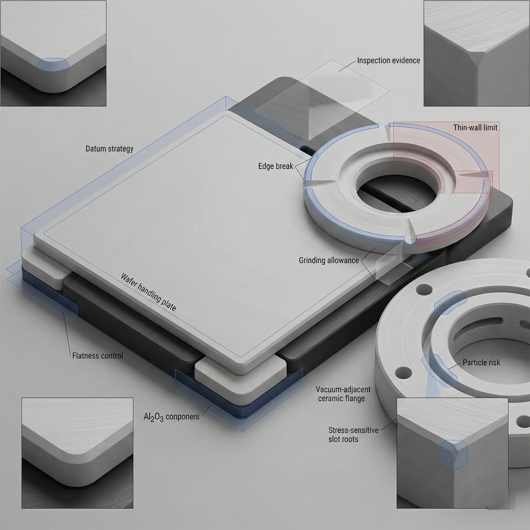
Semiconductor ceramic components are rarely purchased on material name alone. The drawing usually combines wafer-contact geometry, vacuum or gas features, plasma-adjacent edges, thermal interfaces, electrical isolation, or clean assembly requirements. Each functional zone changes the machining and inspection route.
A useful review begins by identifying where the part touches a wafer, seals against another component, controls height or flatness, carries heat, provides insulation, or faces process chemistry. Those zones should drive the datum plan, grinding or lapping scope, edge criteria, cleaning requirement, and evidence package.
This page organizes the existing semiconductor engineering guides by component family. It does not promise that every geometry or tolerance is feasible; final scope depends on the drawing, ceramic grade, blank state, quantity, and agreed acceptance method.
Component families
These are not catalog promises. They are review paths for connecting geometry, material, process, and evidence to the function of the part.
End effectors, lift pins, support fingers, contact pads, and alignment features controlled by flatness, contact height, edge chips, particles, and robot datums.
Dense or porous ceramic plates, groove fields, micro-holes, mounting datums, and working faces reviewed for flatness, suction behavior, cleaning, and protected handling.
SiC or alumina rings, lapped annular bands, IDs, ODs, grooves, holes, and process-side edges where geometry, chemistry, and particle control meet.
Alumina rings, sleeves, spacers, and AlN thermal insulators with creepage paths, bore fits, lapped faces, and plasma-sensitive edge zones.
Micro-bores, orifices, hole arrays, slots, and vacuum passages specified by diameter, depth, taper, breakout, position, cleaning, and inspection access.
AlN plates, heat-spreader interfaces, heater-adjacent parts, clean fixtures, and sensor supports controlled by flatness, thickness, Ra, contamination, and packaging.
Decision map
Use the final column as a drawing and RFQ check. A requirement is easier to review when its function and acceptance evidence are stated together.
| Requirement | Why it changes the route | What to define in the RFQ |
|---|---|---|
| Wafer or process contact zones | Contact height, particles, edge chips, and local finish can affect handling yield or process cleanliness. | Mark contact pads, protected edges, allowable chip zones, finish, and optical acceptance on the drawing. |
| Flatness and datum strategy | Large plates and rings can measure differently when free-state, supported, or clamped in the tool. | State support condition, datum faces, measurement map, temperature, and any assembly preload assumptions. |
| Vacuum and micro-features | Hole taper, breakout, blocked passages, groove edges, and cleaning residue can change functional behavior. | Provide hole geometry, flow or vacuum boundary, cleanliness target, and whether functional testing is required. |
| Cleaning and packaging | A dimensionally acceptable ceramic part can still fail incoming inspection because of particles, residue, or transit chips. | Define final cleaning, handling, bagging, contact protection, labeling, and lot traceability expectations. |
Material paths
Common for electrical insulation, chamber hardware, spacers, rings, feedthrough-adjacent parts, and cost-sensitive clean components. State purity and grade.
Considered for stiff, wear-resistant, chemically stable wafer-handling and process-side hardware. Blank route and finished feature risk need review.
Used when electrical isolation and thermal transfer must coexist. Thermal faces, thickness, edge condition, and moisture-sensitive handling require clear notes.
Zirconia, silicon nitride, Macor, BN, porous ceramics, and customer-specified grades may fit specific fixtures, prototypes, thermal, vacuum, or flow functions.
Quote-ready package
Engineering guides
Each guide below narrows one part family or manufacturing constraint and leads back to the drawing information needed for review.
Engineering guide to precision ceramic components for semiconductor equipment, including wafer handling parts, vacuum chucks, SiC rings, AlN plates, alumina insulators, micro-hole parts, tolerances, surface finish, inspection, and RFQ inputs.
How to source silicon carbide wafer-handling parts, including end effectors, lift pins, support pads, contact zones, edge criteria, cleaning, and inspection.
Choose and specify ceramic wafer end effectors by contact mode, material, fork geometry, robot interface, vacuum features, edge quality, and inspection.
Review ceramic vacuum chuck components for semiconductor tools: pressure boundary, dense or porous construction, replacement interfaces, flatness, and functional acceptance.
Engineering guide to precision ceramic rings for semiconductor process chambers, including SiC and alumina ring components, lapped bands, ID/OD control, grooves, edge quality, cleaning, inspection, and RFQ inputs.
Engineering guide to ceramic insulators for plasma etching and deposition equipment, including alumina rings, AlN thermal insulators, feedthrough sleeves, spacers, creepage paths, lapped faces, edge quality, cleaning, inspection, and RFQ inputs.
Design and RFQ guide for ceramic nozzles used in semiconductor, vacuum, dispensing, gas flow, and clean equipment, including material selection, micro-bore geometry, edge quality, cleaning, and inspection.
Engineering guide to aluminum nitride ceramic parts for semiconductor thermal management, including AlN heat spreaders, heater-adjacent plates, flatness, Ra, cleaning, packaging, inspection evidence, and RFQ review.
RFQ-ready engineering guide for precision machined alumina ceramic parts used in semiconductor processing equipment, including insulating rings, feedthrough sleeves, nozzles, gas plates, spacers, lapped faces, cleaning, packaging, supplier capability questions, and inspection evidence.
Engineering RFQ guide for precision ceramic components used in cleanroom and high-purity manufacturing systems, covering alumina, zirconia, SiC, AlN, nozzles, sleeves, spacers, rings, plates, cleaning, packaging, inspection evidence, and qualification boundaries.
Questions before quotation
Alumina, silicon carbide, aluminum nitride, silicon nitride, zirconia, Macor, BN, and porous ceramics may be reviewed. The correct route depends on electrical, thermal, chemical, stiffness, wear, cleanliness, blank, and feature requirements.
A STEP file helps geometry review, but a useful quotation also needs material grade, quantity, functional datums, critical surfaces, edge criteria, cleaning, packaging, inspection method, and application context.
Identify the functional face, datum or support condition, free-state or clamped measurement condition, temperature, mapping method, excluded edge band, and required report. Feasibility is confirmed after drawing and blank review.
Include material or operating environment, quantity, target timing, functional surfaces, tolerance and finish priorities, cleaning, packaging, and inspection evidence. Feasibility, price, and lead time are confirmed after review.