Published · Updated · CERAMIC CNC Engineering · Engineering Guide · 8 min read
SiC Wafer Handling Parts: Design, Machining, and RFQ
How to source silicon carbide wafer-handling parts, including end effectors, lift pins, support pads, contact zones, edge criteria, cleaning, and inspection.
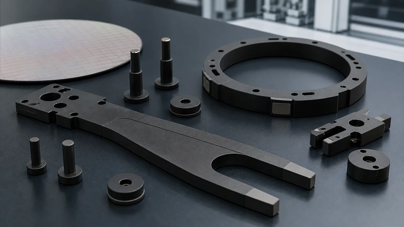
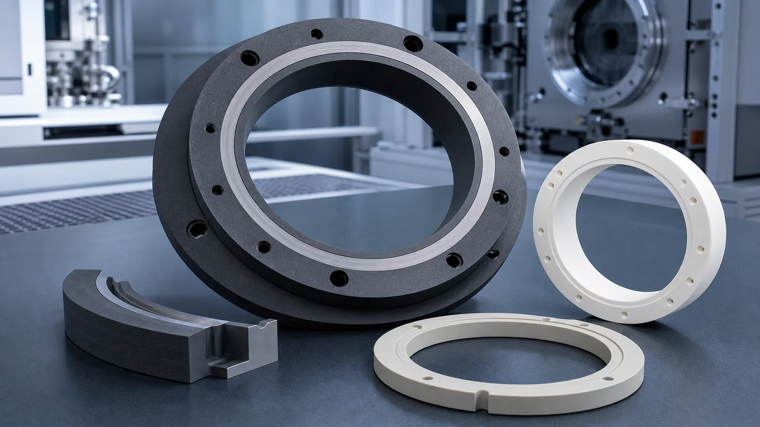
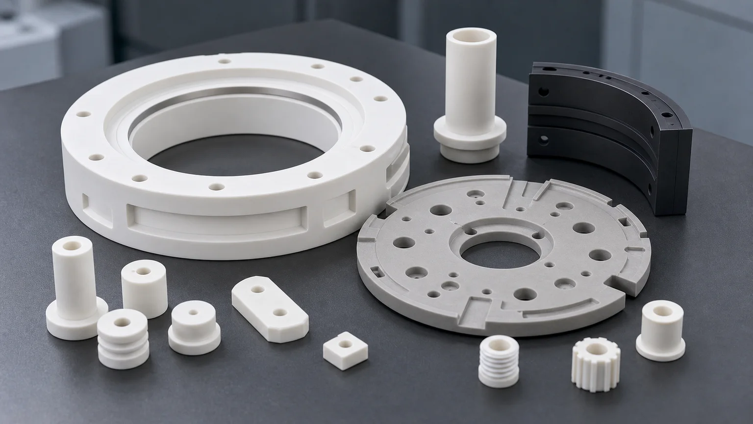
A silicon carbide wafer-handling part should be specified as a controlled contact interface, not as a generic SiC shape. Mark where the wafer touches, which datums locate the part, which edges are particle-sensitive, how the component will be cleaned, and what evidence will prove acceptance.
This page is for equipment engineers and buyers who already have a silicon carbide direction and need machined end effectors, lift pins, support pads, carrier segments, support rings, or related semiconductor-tool parts. If the material is still open, compare the material-neutral ceramic wafer end-effector guide first.
What Counts as a SiC Wafer-Handling Part?
| Part family | Function | Features that usually control the quote |
|---|---|---|
| End-effector blade or fork | Transfers or supports a wafer | Arm thickness, contact pads, profile, mounting datums, edge chips |
| Lift pin or support pin | Raises, lowers, or locates a wafer | Tip geometry, set height, straightness, runout, protected packaging |
| Contact pad or support block | Provides local support | Lapped area, height, parallelism, edge radius, cleanliness |
| Carrier segment or support ring | Supports a circular substrate or fixture | Flatness, concentricity, support band, holes, slots, cleaning |
| Edge-contact element | Locates or grips a wafer or carrier | Contact radius, local finish, chip limit, wear zone, assembly fit |
| Metrology or handling fixture | Holds a wafer or component during inspection | Datum strategy, support pattern, bore position, repeatability evidence |
This article concerns equipment components made from SiC. It is not about manufacturing SiC semiconductor wafers themselves.
Why SiC Is Considered for Wafer Handling
Silicon carbide may be selected where a handling component needs a useful combination of stiffness, wear resistance, thermal stability, chemical stability, and clean process-side behavior. Saint-Gobain lists wafer grinding and polishing plates, vacuum-chuck discs, wafer clamps, and wafer carriers among semiconductor applications for a sintered SiC grade. CoorsTek also shows ceramic end effectors and SiC lift pins in wafer-handling applications.
Those examples establish that SiC is used in this equipment class; they do not make every grade interchangeable or every design suitable. The RFQ should still state:
- Exact SiC grade or approved material reference.
- Whether equivalent-grade review is allowed.
- Density, purity, certificate, and lot-traceability expectations where applicable.
- Blank form and whether the blank is customer-supplied or supplier-sourced.
- Process exposure: vacuum, gas, cleaning chemistry, temperature, thermal cycling, or plasma-adjacent service.
- Qualification stage: prototype, replacement part, validation lot, or released production design.
If the material is not locked by a qualified tool design, provide the operating requirements rather than asking for unspecified “high-purity SiC.”
Four Control Zones on the Drawing
1. Wafer-contact zone
Identify every pad, tip, band, or edge that can touch the wafer. For each zone, define the contact mode and the geometry that matters:
- Underside support, edge contact, temporary lift, or vacuum-assisted hold.
- Contact area and location.
- Flatness, profile, parallelism, or matched height.
- Surface finish on the contact area only.
- Edge break, radius, chamfer, or maximum chip size.
- Whether marks, residue, or visual defects are permitted.
A blanket polish note can add cost to nonfunctional faces while leaving the real contact zone unclear.
2. Robot or tool-interface zone
The part must return to the same coordinate system after installation. Mark the primary mounting face, bores, slots, dowel locations, shoulders, and other features that establish position. State whether the part is clamped, fastened, bonded, or assembled into a metal holder and provide preload or torque context when known.
3. Particle-sensitive edge zone
“No chips” is not an inspectable acceptance criterion. Separate wafer-facing tips, slot edges, hole rims, mounting edges, and nonfunctional outside edges. Define a practical visual standard for each critical zone, including magnification and maximum allowable chip size when needed.
4. Cleaning and packaging zone
Finished SiC surfaces can pass dimensional inspection and still be damaged or contaminated afterward. Define final cleaning, handling, bagging, separators, trays, labeling, lot control, and protection for tips or lapped pads.
Design Review by Component Type
SiC end effectors and blades
Long arms and narrow forks combine stiffness requirements with machining and handling risk. Review unsupported length, blade thickness, fork width, slot radius, arm-to-body transition, hole-to-edge distance, contact-pad location, moving mass, and mounting relationship. Sharp internal corners and thin metal-style webs should be challenged before the drawing is frozen.
Use the ceramic DFM rules for slots, pockets, counterbores, thin sections, and edge relief. The separate ceramic end-effector guide compares SiC with alumina, zirconia, silicon nitride, and machinable-ceramic options when material selection is still open.
SiC lift pins and support pins
For a pin set, the top contact geometry and height relationship may matter more than nominal diameter. Specify tip shape, tip finish, shoulder, length, straightness or runout, set matching, and whether an individual pin can be replaced independently. Packaging should prevent tip-to-tip contact.
SiC support rings and carrier parts
For circular support parts, identify the actual support band rather than applying the tightest finish to the full face. Review support-band flatness, ID/OD relationship, concentricity, groove and hole position, lapped zones, and free-state versus supported inspection. The semiconductor process-ring guide covers ring-specific datum and inspection choices.
Vacuum or flow features
Small holes, grooves, and passages can dominate the route because diameter, depth, taper, breakout, debris, and blockage all matter. State whether dimensional inspection is sufficient or whether flow, leakage, or functional vacuum evidence is required. Use the ceramic micro-hole RFQ guide and the ceramic vacuum-chuck guide when those features drive the design.
Tolerance and Inspection Plan
Avoid assigning one tolerance class to the complete component. Build an acceptance table around functional features.
| Requirement | Inspection question | Possible evidence to agree |
|---|---|---|
| Contact-pad flatness or set height | Is the part measured free-state, supported, or in a fixture? | Flatness map, CMM, optical method, or matched-set report |
| Mounting bore or slot position | Which finished faces establish the datum system? | CMM, fixture gauge, or key-dimension report |
| Blade or fork profile | How are long thin sections supported during measurement? | Optical profile, CMM, scan, or functional fixture |
| Edge-chip control | Which edges are critical and at what magnification? | Zone-based visual report or approved reference standard |
| Contact-surface finish | Which small faces need Ra or lapping? | Surface-roughness result or process/inspection record |
| Pin tip geometry and set match | Is acceptance individual or as a matched set? | Height, radius, runout, and set-identification report |
| Hole or vacuum feature | Is geometry or function the acceptance gate? | Optical check, pin gauge, flow check, or leakage test |
| Cleaning and packaging | What must be protected after inspection? | Cleaning note, packaging standard, and incoming visual plan |
The ceramic tolerance capability map helps connect each callout to a machining and measurement method. Final values still require grade, size, geometry, and blank review.
What Usually Drives Cost and Lead Time?
For SiC wafer-handling parts, price is rarely proportional to outside size alone. Major drivers include:
- Exact SiC grade, blank availability, certificate, and qualification restrictions.
- Fired-state removal and diamond-tool time.
- Long arms, narrow slots, thin sections, and low-yield edge geometry.
- Lapped or controlled-finish contact pads.
- Mounting-datum position relative to wafer-contact surfaces.
- Matched lift-pin or support-pad sets.
- Visual edge acceptance in particle-sensitive zones.
- Cleaning, individual protection, and controlled packaging.
- Flatness, CMM, optical, surface, or functional test reports.
- Prototype learning and customer qualification before repeat production.
The most productive cost review is to tighten the wafer-contact and alignment features while using standard finish and edge acceptance on true clearance areas.
Quote-Ready SiC Wafer-Handling RFQ
Send the following in one package:
- 2D drawing with revision plus STEP or native CAD.
- Part type and function in the semiconductor tool.
- Exact SiC grade, approved equivalent rule, blank source, and certificate needs.
- Wafer or substrate size, contact mode, and supported area.
- Wafer-contact faces, particle-sensitive edges, datums, and mounting interfaces marked on the drawing.
- Flatness, profile, height match, bore position, surface finish, and edge criteria by functional zone.
- Holes, slots, grooves, vacuum passages, and thin sections called out completely.
- Cleaning, packaging, traceability, and inspection-report requirements.
- Prototype and production quantity, target timing, and qualification stage.
If a requirement is unknown, label it as open. A supplier can then return a focused clarification instead of silently pricing an assumption. The general ceramic RFQ checklist provides a reusable submission structure, and the RFQ page is the conversion point for a drawing review.
Common Questions
Why use SiC instead of alumina for a wafer-handling part? SiC may be selected for stiffness, wear, thermal stability, chemical stability, or a qualified clean process route. Alumina may be more practical where electrical insulation, availability, or cost dominates. Compare exact grades and functions rather than material names alone.
Can a SiC end effector be quoted from a STEP file? A STEP file can start geometry review, but a reliable quote also needs the material grade, contact zones, datums, surface requirements, edge criteria, quantity, cleaning, packaging, and inspection plan.
Should every face be polished? No. Apply lapping or controlled finish to contact, sealing, sliding, or datum surfaces that need it. Nonfunctional clearance faces usually do not need the same treatment.
What is the most important drawing note? There is no single note. The highest-value information is a marked relationship among wafer-contact zones, mounting datums, particle-sensitive edges, and the method used to inspect them.
Technical References
- Saint-Gobain: silicon carbide components for wafer handling and inspection
- CoorsTek: processing and wafer-handling ceramic components
RFQ note: Final material, tolerance, price, lead time, cleaning, packaging, and inspection scope depend on drawing review, SiC grade, blank state, quantity, process route, and agreed acceptance criteria.
- Silicon carbide
- Wafer handling
- Semiconductor ceramics
- SIC components
- Contact surfaces
- Clean packaging
- Inspection
- RFQ checklist