Published · CERAMIC CNC Engineering · Engineering Guide · 8 min read
Machined Ceramic Plates for RF and Microwave Assemblies
RFQ guide for machined alumina, AlN, and other ceramic plates used in RF and microwave assemblies, including flatness, thickness, holes, finish, and inspection.

An RF or microwave ceramic plate should be quoted from the electrical design and mechanical interface together. The customer specifies the approved dielectric material and validates circuit performance; the machining RFQ converts that design into measurable thickness, flatness, holes, pockets, edge condition, surface finish, cleaning, and inspection requirements.
This guide is for engineers sourcing custom ceramic plates, carriers, spacers, window blanks, support blocks, or fixture components used in RF and microwave assemblies. It focuses on precision machining and acceptance to print. It does not claim to design or certify an RF circuit, antenna, resonator, metallization system, or finished electronic module.
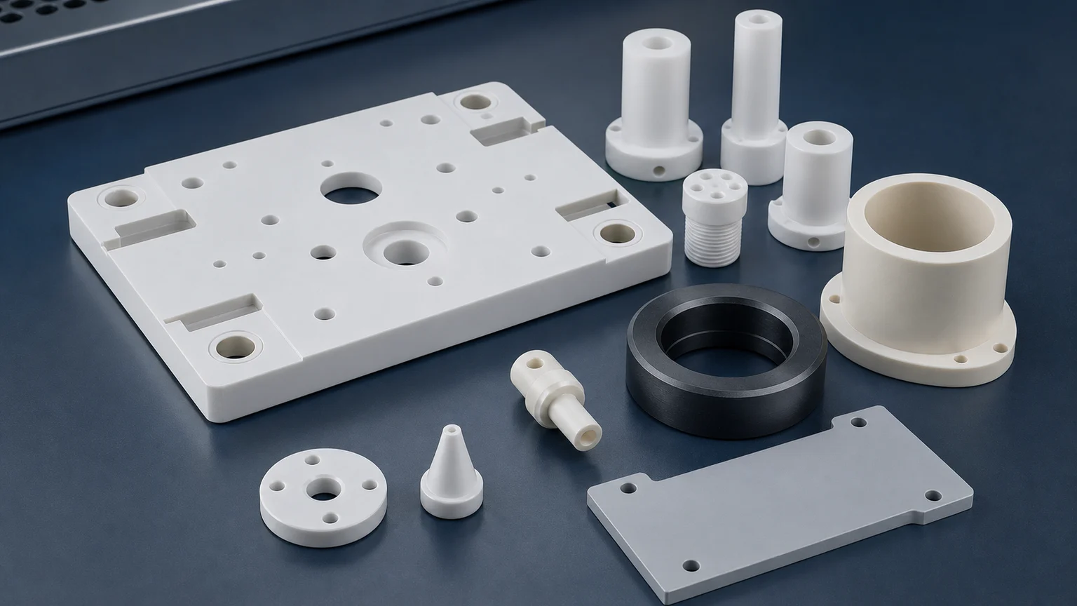
Parts Covered by This Machining Scope
| Component family | Mechanical function | RFQ features that commonly matter |
|---|---|---|
| Ceramic substrate or carrier plate | Supports thin-film, thick-film, hybrid, or mounted components | Thickness, flatness, parallelism, surface finish, outline, holes, edge quality |
| Insulating spacer or standoff plate | Sets dielectric spacing and separates conductive hardware | Thickness, bore position, creepage geometry, edge radius, assembly fit |
| RF window or dielectric blank | Provides a customer-designed dielectric interface or barrier | Grade, thickness map, parallelism, surface condition, edge seal geometry |
| Cavity support or alignment plate | Locates conductors, packages, ferrites, absorbers, or modules | Datum system, pocket depth, hole position, slot width, profile |
| Waveguide or feedthrough-adjacent insert | Provides insulation or dielectric geometry in an assembly | Bore, concentricity, sealing shoulder, edge condition, metallization boundary |
| Test and tuning fixture plate | Holds RF components during assembly, inspection, or characterization | Repeatable datums, locating pins, flat support areas, replaceable contact zones |
If the requirement is a fully metallized circuit substrate, co-fired package, filter, antenna, or qualified microwave window, state which operations are customer-controlled and which are included in the ceramic machining scope.
Material Must Come From the RF Design
Do not select a ceramic grade from a generic property table alone. Dielectric constant, loss, temperature behavior, thermal conductivity, coefficient of thermal expansion, purity, surface condition, and metallization compatibility can all matter. Use the exact approved grade and its lot or certificate requirements when the electrical design is already qualified.
| Material direction | Where it may fit | Machining and RFQ caution |
|---|---|---|
| High-purity alumina | RF/MIC substrates, insulating plates, spacers, carriers, and window blanks | Specify purity and supplier grade; post-fired holes, profiles, lapping, and edge finishing may be required |
| Aluminum nitride (AlN) | Plates that combine electrical isolation with stronger heat spreading | Identify thermal faces, moisture-handling rules, thin sections, edge risk, and metallization sequence |
| Macor or machinable glass ceramic | Prototype fixtures, insulating supports, and fast geometry iterations | Use only when its dielectric, thermal, vacuum, and mechanical limits fit the design |
| Fused silica, quartz, sapphire, or customer-qualified ceramic | Specialized low-loss, optical, thermal, or environmental designs | Confirm the supplier’s actual material and process scope; do not assume alumina methods transfer directly |
| Proprietary dielectric ceramic | Resonators, filters, and frequency-specific components | Grade, orientation, fired blank, tuning allowance, and electrical validation must come from the design owner |
Kyocera identifies high-purity 99.6% alumina as an option for microwave integrated-circuit substrates, and CoorsTek describes ceramic substrates for thin-film and thick-film applications extending into high-frequency microwave use. These are examples of qualified material systems, not permission to substitute one alumina grade for another.
Use the ceramic material selection guide for an early mechanical screening, then return to grade-specific electrical data before release.
Separate RF Performance From Machining Acceptance
The most important scope decision is who owns each result.
The design owner normally controls and validates:
- Dielectric constant and loss target at the relevant frequency and temperature.
- Electromagnetic geometry, impedance, resonance, insertion loss, isolation, and power handling.
- Metallization stack, adhesion, conductor pattern, brazing, bonding, plating, and circuit qualification.
- System-level thermal, vacuum, pressure, and electrical testing.
The ceramic machining RFQ can control:
- Material identity and blank traceability within the agreed supply scope.
- Overall dimensions, thickness, flatness, parallelism, profile, bores, holes, slots, and pockets.
- Surface finish on named faces.
- Edge radius, chamfer, breakout, and chip criteria.
- Cleaning, handling, protected packaging, and dimensional evidence.
Keeping this boundary explicit prevents a dimensionally acceptable ceramic blank from being treated as proof of final RF performance.
Dimensions That Usually Matter Most
Thickness and parallelism
Thickness may be part of the electromagnetic design, the mechanical stack, or both. Specify nominal thickness, local tolerance, whether a map is required, and the relationship between opposite faces. A single corner measurement may not prove a large plate.
Flatness and support condition
Flatness can affect bonding, clamping, thermal contact, assembly gaps, and conductor processing. State whether the plate is measured free-state, on a reference surface, or in a customer fixture. Define the usable area and any excluded edge band.
Hole, slot, and pocket position
Mounting holes, vias, feedthrough openings, device pockets, and tuning-access features should reference stable datums. State diameter, depth, taper, entry and exit condition, internal radius, hole-to-edge distance, and inspection method.
Surface finish
Tie finish to the operation that follows. A face prepared for thin-film processing, bonding, metallization, thermal contact, or sealing may need different control from a clearance surface. Do not specify “polish all over” unless the complete surface is functional.
Edge condition
RF plates are vulnerable at corners, hole exits, slots, and thin sections. Define a controlled edge break and zone-based chip criteria. An undefined sharp edge is both a handling risk and an unreliable inspection requirement.
For feature-specific process planning, use the ceramic tolerance capability map and surface finish and subsurface damage guide.
Choosing the Machining Sequence
The sequence depends on blank state, geometry, quantity, and downstream processing.
| Sequence question | Why it changes the quote |
|---|---|
| Is the plate machined green, as-fired, or fully fired? | Sintering can change final dimensions; hard finishing adds precision but also time and edge risk |
| Are the major faces lapped before or after holes and profiles? | Later operations can affect flatness, edge condition, and cleanliness |
| Does metallization happen before or after final machining? | Clamping, coolant, heat, edge removal, and masking can damage or alter finished metallization |
| Are pockets and holes produced by grinding, laser, ultrasonic, or another approved method? | Feature size, depth, taper, heat-affected risk, edge quality, and cost differ |
| Is final cleaning compatible with the next process? | Residue limits and handling rules depend on bonding, metallization, vacuum, or clean assembly needs |
If metallization is already present, provide keep-out zones, allowable contact surfaces, masking, coolant restrictions, and cosmetic/functional damage criteria. If metallization is downstream, identify the surface preparation and packaging condition required by that process owner.
DFM Questions for Ceramic RF Plates
Review these before releasing the drawing:
- Can sharp internal corners become practical radii?
- Is there enough material between holes, slots, pockets, and outside edges?
- Are thin islands or webs supported during machining and inspection?
- Does every tight dimension affect RF, assembly, thermal contact, or sealing?
- Can one finished face serve as the primary datum?
- Are depth and corner requirements compatible with tool access?
- Is the blank available near the requested size and thickness?
- Can the part be handled without touching a critical face or metallized area?
The ceramic CNC machining design rules cover corner radii, thin walls, holes, pockets, and edge distances in more detail.
Inspection Evidence to Request
| Requirement | Evidence to discuss |
|---|---|
| Material and grade | Certificate, lot identification, or customer-supplied blank record |
| Thickness and parallelism | Thickness map, comparator, micrometer plan, or CMM report |
| Flatness | Optical, mechanical, CMM, or agreed map under a defined support condition |
| Hole and pocket position | CMM, optical inspection, pin gauge, or fixture gauge |
| Surface finish | Ra or other agreed result on the named face and direction |
| Edge quality | Zone-based visual inspection with defined magnification and chip limit |
| Cleanliness and protection | Cleaning note, approved packaging, separators, and face protection |
Electrical characterization should be specified separately if it is required. Do not assume a standard dimensional report includes dielectric, RF, metallization, adhesion, leak, or thermal testing.
Quote-Ready RF and Microwave Ceramic Plate RFQ
Send:
- Controlled 2D drawing plus STEP or native CAD.
- Part function and assembly position, without disclosing unnecessary proprietary system details.
- Exact material manufacturer, grade, purity, blank source, and substitution rule.
- Frequency, thermal, vacuum, and electrical context needed to understand manufacturing risk.
- Functional faces, RF-sensitive dimensions, thermal contacts, sealing zones, and assembly datums marked clearly.
- Thickness, flatness, parallelism, holes, slots, pockets, finish, and edge criteria by feature.
- Metallization status, process sequence, keep-out zones, and downstream surface-preparation needs.
- Cleaning, packaging, certificate, traceability, and inspection requirements.
- Prototype and production quantity, target timing, and qualification stage.
The alumina electrical-insulator guide is useful for creepage, bore, and mounting geometry. For heat-spreading plates, use the AlN machining guide and AlN heat-spreader guide. Submit a controlled drawing package through the technical RFQ page.
Common Questions
Which ceramic is best for RF and microwave plates? There is no universal best material. The electrical design must select an exact grade from dielectric, loss, thermal, mechanical, metallization, environment, availability, and qualification requirements.
Can an RF ceramic plate be CNC machined after firing? Many fired technical ceramics can be precision finished using diamond grinding, lapping, laser processing, ultrasonic machining, or other specialist methods. The feature and material determine the route.
Does tighter flatness always improve RF performance? Not automatically. Flatness may affect assembly, bonding, interfaces, and some electrical geometries, but the design owner should define the value and validate system performance. Unnecessary tight flatness adds machining and inspection cost.
Can metallized ceramic be machined? Sometimes, but the sequence needs review. Existing metallization can be damaged by fixturing, coolant, heat, edge removal, or cleaning. Provide the metallization stack, keep-out zones, and acceptance criteria before quotation.
What should be sent for a first review? Send the drawing, CAD, exact material grade, blank or metallization status, quantity, functional faces, critical dimensions, surface and edge requirements, downstream process, and inspection needs.
Technical References
- Kyocera: high-purity alumina microwave integrated-circuit substrates
- CoorsTek: thin-film and thick-film electronic ceramic substrates
RFQ note: Final material, feature feasibility, tolerance, price, lead time, cleaning, packaging, and inspection scope depend on drawing review, exact grade, blank state, quantity, process sequence, metallization status, and agreed acceptance criteria.
- RF ceramics
- Microwave components
- Ceramic plates
- Alumina
- Aluminum nitride
- Flatness
- Surface finish
- RFQ checklist